2015年6月18日星期四

How To Find A Good PCB Supplier

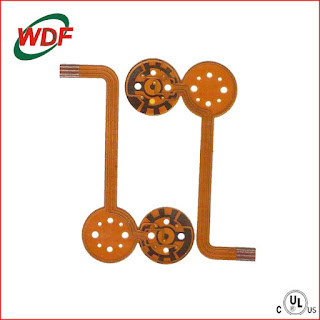
Flexible PCB( WDF-FPC-D-18 ) - wonderfulpcb.com


A famous star need a good director, if Jack Chen or Tom Hanks, or Nicolas Cage met with a mediocre director, I guess the box office would take a tumble.
Just like to find a good director for a movie, if you are purchasing for PCB circuit boards, you need to find a good PCB supplier firstly.

Here are some proven tips to guide you through the selection process successfully.

Market Orientation: 

Carrying out a background research on the different suppliers will help you know the exact price that you should pay for the services to be rendered. Understanding market orientation can also help you find quality services. Note that each PCB supplier specializes in one field that he or she is good at.

Manufacturing criteria: 

What is cared most often is the manufacturing criteria of PCB supplier, his/her production capacity, lead-time, quality, and service. If a PCB supplier only have a low production capacity, your purchasing requirements may not be satisfied, for example, you need to produce a multilayer board while technology and devices of the supplier are backward and couldn’t take this order. Punctual lead-time is one of points to be considered, it is related with production capacity but also related with management system of the PCB supplier. A superior management system will greatly improve production efficiency. At last, a good service also is essential which includes prompt reply, good communication, and settlements for the quality issues.  

Desist from choosing PCB suppliers who offer low prices. Instead, you should find suppliers whose prices are directly proportional to the quality of the products. Sometimes, low quality products are very cheap as compared to high quality products. One of the major benefits of purchasing a high quality product is that they are more cost effective since they are more durable hence they require less repair or maintenance services.

Finally, find companies that have a clean track record so as to get value for your money. Their repairing costs should be affordable and in line with your budget. Once your products have passed the R & D, find a reliable partner who can help you establish and expand your market and credibility.

A PCB supplier in Shenzhen of China which you must be interested in:
http://www.wonderfulpcb.com

2015年5月25日星期一

"Afternoon Tea": The first train technical talents for PCB industry school founded in Suining


PCB industry is the national "twelfth five-year" emerging strategic industries, high gold content technology, and technical skill talent gap more than 400000 people a year. Facing with the situation of skills talents shortage in suining, British creativity and thoughts of the school. In 2014, the state council issued "about speed up the development of modern vocational education decision", to "deepen the integration production and education, to encourage industry enterprises organize or participate in vocational education, give play to the role of enterprise important governance subject”. The open area at the same time vigorously called for a "public entrepreneurship, people’s innovation", more strengthened the faith that enterprise education. Earlier this year, the company has formed a "suining British chuangli printing technical vocational school" education plan, and get the support of municipal party committee, municipal government and the open area, the city bureau of education, city people club bureau with efficient service power enterprises."We have the confidence to the learned school-run me!"YiKeHua said.

The creativity of educational philosophy

On the concept of operations, the creativity and proposed "the CDB area economic development by service, service students' lifelong development, service PCB industry development for the purpose, committed to the development with international vision and international standard of PCB industry technical elite, the industry leader" of the training objectives, to build "the government, industry, enterprise, school, four one" training mode, the innovation "the school cooperation, JiaoJiao cooperation, cooperation, international cooperation between higher vocational colleges and the school-running idea, to create enterprise as" teaching management, teaching content, post production, project teaching method, teaching process and teaching information, teaching standard internationalization "school characteristics.

The creativity of education foundation

The creativity and the southwest university of science and technology, chengdu university of electronic science and technology and other institutions to carry out the cooperation between colleges and the talent training scheme between the two sides make joint the PCB industry, develop the school-based curriculum in the PCB production technology and participate in the teaching process. At present, the creativity and become students practice and high salary employment entrepreneurial base oral confession, three years has more than 500 people develop technical skills talents. Recently, the suining chuangli electronic technology co., LTD., is listed as one of the chengdu university of electronic science and technology postdoctoral workstation and PCB engineering experiment and scientific research achievements transformation base in Sichuan province.

2015年5月7日星期四

The Advantages and Disadvantage of FPC

FPC, Flexible PCB


A: Disadvantages:
1. Original cost is high
Because the FPC is designed and made for special application, the cost of circuit design, wiring and photographic plate is high. Except special need, we’d better not use them.

2. The modification and correction is difficult
Once FPCs are made, if we want to modify, we have to begin from the base drawing or gerber program. Therefore it’s difficult to change. On its surface there is a coverlay. Before the modification, we have to remove it, after the modification, we have to recover it, which is difficult.

3. Dimension limitation
Since FPC is not popular, we usually use intermittent method to make them. Then we can’t make too long or wide FPC with the limit of manufacture instruments dimensions.

4. Easier to be damaged if improper operation
It is easier to cause the damage of FPC circuits because of improper operation. Special trained workers are needed in tin plating and rework

B: Advantages
FPC is the printed circuit board which is made of flexible insulating base material. It has many advantages many rigid PCBs don’t have.

1. It can be bent, rolled, folded freely, can be arranged randomly according to the space, can be moved and stretched in 3-D space, then integrate the components assembly and wiring connection.

2. It can satisfy the need of electronic products to develop in the direction of high density, smaller size, higher reliability, since FPC can greatly reduce the volume and weight of electronic products. Therefore FPC is widely applied in fields or products of aerospace, military, mobile communication, laptop, computer exterior design, PDA, and digital camera.

3. FPC also has the advantages of good thermal diffusivity and solderability, easy to assembly, low combined cost. The design of rigid-flex boards also make up the disadvantage of components carrying ability of flexible base material.

If you need expert FPC service, feel free to contact wonderful02@wonderfulpcb.com

2015年4月15日星期三

Printed Circuit Board

A printed circuit board, or PCB, is a self-contained module of interconnected electronic components found in devices ranging from common beepers, or pagers, and radios to sophisticated radar and computer systems. The circuits are formed by a thin layer of conducting material deposited, or "printed," on the surface of an insulating board known as the substrate. Individual electronic components are placed on the surface of the substrate and soldered to the interconnecting circuits. Contact fingers along one or more edges of the substrate act as connectors to other PCBs or to external electrical devices such as on-off switches. A printed circuit board may have circuits that perform a single function, such as a signal amplifier, or multiple functions.
There are three major types of printed circuit board construction: single-sided, double-sided, and multi-layered. Single-sided boards have the components on one side of the substrate. When the number of components becomes too much for a single-sided board, a double-sided board may be used. Electrical connections between the circuits on each side are made by drilling holes through the substrate in appropriate locations and plating the inside of the holes with a conducting material. The third type, a multi-layered board, has a substrate made up of layers of printed circuits separated by layers of insulation. The components on the surface connect through plated holes drilled down to the appropriate circuit layer. This greatly simplifies the circuit pattern.
Components on a printed circuit board are electrically connected to the circuits by two different methods: the older "through hole technology" and the newer "surface mount technology." With through hole technology, each component has thin wires, or leads, which are pushed through small holes in the substrate and soldered to connection pads in the circuits on the opposite side. Gravity and friction between the leads and the sides of the holes keeps the components in place until they are soldered. With surface mount technology, stubby J-shaped or L-shaped legs on each component contact the printed circuits directly. A solder paste consisting of glue, flux, and solder are applied at the point of contact to hold the components in place until the solder is melted, or "reflowed," in an oven to make the final connection. Although surface mount technology requires greater care in the placement of the components, it eliminates the time-consuming drilling process and the space-consuming connection pads inherent with through hole technology. Both technologies are used today.
Two other types of circuit assemblies are related to the printed circuit board. An integrated circuit, sometimes called an IC or microchip, performs similar functions to a printed circuit board except the IC contains many more circuits and components that are electrochemically "grown" in place on the surface of a very small chip of silicon. A hybrid circuit, as the name implies, looks like a printed circuit board, but contains some components that are grown onto the surface of the substrate rather than being placed on the surface and soldered.
Wonderful PCB (HK) Limited, with over 15 years experience of producing PCB, fabricates printed circuit boards for customers in many industries worldwide, including communications/telecom/IT, medical electronics, consumer electronics (mobile phones, computers, LED lighting, etc.), and the automobile industry. We supply high-precision, high-density, double-sided and multilayer custom PCBs and PCBA services for customers in many countries.

About PCB service

1. Installation and welding of parts
the last step is the installation and welding the parts. Both THT and SMT parts use of machinery and equipment to install is placed on the PCB.
THT parts are usually called the Wave Soldering (Wave Soldering) way of welding. This allows all parts to a welding on the PCB.First to pin cut close to the board, and slightly bent so that parts can be fixed. Then the PCB will be moved to the co solvent on the waves of make contact to help at the bottom of the solvent, it can be on the base metal of the oxide to get rid of. After the heated PCB, the move to the melting of solder, at the bottom and contact after welding is completed.
Automatic welding of SMT parts way is called to flow back to welding (Over Reflow Soldering).Contains co solvent and solder paste in welding, the parts installed on the PCB after the first treatment time, was a PCB again after heating treatment. For PCB cooling after welding is completed, the next is to prepare the final test of PCB board.

2. Proofing
PCB's Chinese name is called printed circuit board, also known as printed circuit boards; printed circuit board is an important electronic component is electronic components support body? The provider of the electrical connection in the electronic components. Because it is made of so called electronic printing "printed circuit board.
PCB proofing is refers to the pilot production of printed circuit board before mass production is mainly used for electronic engineers in the design of circuit? And complete the PCB Layout to the factory after small batch trial-produce process is the PCB proofing. And PCB proofing production quantity generally no specific boundary is an engineer in product design has been finished to confirm and complete the test before we call it PCB proofing.

2015年4月13日星期一

Flex circuits

Flex circuits are often used as connectors in various applications where flexibility, space savings, or production constraints limit the serviceability of rigid circuit boards or hand wiring. A common application of flex circuits is in computer keyboards; most keyboards use flex circuits for the switch matrix.
In LCD fabrication, glass is used as a substrate. If thin flexible plastic or metal foil is used as the substrate instead, the entire system can be flexible, as the film deposited on top of the substrate is usually very thin, on the order of a few micrometres.
Organic light-emitting diodes (OLEDs) are normally used instead of a back-light for flexible displays, making a flexible organic light-emitting diode display.
Most flexible circuits are passive wiring structures that are used to interconnect electronic components such as integrated circuits, resistor, capacitors and the like, however some are used only for making interconnections between other electronic assemblies either directly or by means of connectors.
In the automotive field, flexible circuits are used in instrument panels, under-hood controls, circuits to be concealed within the headliner of the cabin, and in ABS systems. In computer peripherals flexible circuits are used on the moving print head of printers, and to connect signals to the moving arm carrying the read/write heads of disk drives. Consumer electronics devices make use of flexible circuits in cameras, personal entertainment devices, calculators, or exercise monitors.
Flexible circuits are found in industrial and medical devices where many interconnections are required in a compact package. Cellular telephones are another widespread example of flexible circuits.
Flexible solar cells have been developed for powering satellites. These cells are lightweight, can be rolled up for launch, and are easily deployable, making them a good match for the application. They can also be sewn into backpacks or outerwear.

If you need expert flexible circuit board service, please contact wonderful02@wonderfulpcb.com.

2015年3月30日星期一

Ball Grid Array

Stands for BGA Ball Grid Array (ball grid array structure PCB), which is an integrated circuit using an organic carrier board an encapsulation method. It has: ① Reduce encapsulation size ② Approve the function, pin count increased ③ PCB board dissolved welding self-centered. ④ high reliability and easy on the tin good electrical properties. ⑤ Low overall cost. BGA PCB board with small holes are more general, most customers BGA vias under design for the finished hole diameter 8 ~ 12mil, BGA paste it into the hole at the surface of the distance to specifications for 31.5mil for example, generally not less than 10.5mil. BGA vias required under the plug hole, BGA pads allow the ink, BGA pads are not bored.

BGA package I / O terminal or columnar joints in a circular distributed in a matrix form underneath the package, BGA technology has the advantage of I / O pin count despite an increase, but the pitch is not reduced but increased to improve assembly yield; although its power increased, but can controlled collapse chip BGA welding method, which can improve its electric performance; thickness and weight compared with the previous packaging technology has decreased; parasitic reduced, signal transmission delay is small, the frequency is greatly improved; assembly can be welded of high reliability. Speaking BGA package without mentioning Kingmax's patented Tiny BGA technology, Tiny BGA

  With the continuous development of science and technology, modern society is closely related with electronic technology, ultra-small mobile phones, ultra-small walkie-talkies, portable computers, memory, hard drives, optical drives, high-definition TV and so on miniaturization, light of the proposed stringent requirements. To achieve reach a goal, we must in the production process, component aspects depth study. SMT (Surface Mount Technology SMT) technology in tune with this trend, for the realization of electronic products, light, thin, short, small foundation.

SMT technology since the 1990s, to a mature stage, but with electronic products, according to the then type / miniaturization, networking and multimedia in the direction of the rapid development of electronic assembly technology put forward higher requirements, the new high-density assembly technologies are emerging, including BGA (Ball Grid Array BGA) is a has entered the practical stage of the high-density assembly technology. This paper attempts to assemble BGA device characteristics and quality control of solder joints to make a presentation.

What is the schematic?

A schematic, or schematic diagram, is a representation of the elements of a system using abstract, graphic symbols rather than realistic pictures. A schematic usually omits all details that are not relevant to the information the schematic is intended to convey, and may add unrealistic elements that aid comprehension. For example, a subway map intended for riders may represent a subway station with a dot; the dot doesn't resemble the actual station at all but gives the viewer information without unnecessary visual clutter. A schematic diagram of a chemical process uses symbols to represent the vessels, piping, valves, pumps, and other equipment of the system, emphasizing their interconnection paths and suppressing physical details. In an electronic circuit diagram, the layout of the symbols may not resemble the layout in the physical circuit. In the schematic diagram, the symbolic elements are arranged to be more easily interpreted by the viewer.
Schematics and other types of diagrams, e.g.,

Contact: Francis WEN
Email address: wonderful06@wonderfulpcb.com
Skype: wonderfulpcb-23

2015年3月22日星期日

WonderfuI Printed Circuit Board

     On the insulating substrate, according to a predetermined design, made of printed wiring assemblies, printer, or combination of both conductive patterns, known as a printed circuit. On the insulating substrate, the electrical connection between the conductive patterns provided components, known as printed wiring. It does not include printed components. Printed circuit or printed circuit board called the finished printed circuit board, or PCB, also known as printing plates used in printing plates in accordance with rigid or flexible substrates can be divided into two categories: rigid printed scrubbing brush and a flexible printed board. this is also Rigid-flex pcb has occurred according to the conductor pattern layers can be divided into single-sided, double-sided and multilayer printed board and the entire outer surface of the conductor pattern surface of the substrate on the same plane printed board, called flat printing plate.
     After the electronic equipment used printing plates, printing plates because of similar consistency, thus avoiding the manual wiring errors, and can realize automatic insertion of electronic components or mount, automatic soldering, automatic testing to ensure the quality of the electronic equipment to improve labor productivity, reduce costs, and ease of maintenance. printing plates from development to single-sided, multi-layer and flexible, and still protect the respective trends. due to continuous high-precision, high density and high reliability direction, shrinking volume, reduce costs, making printing plates in the future development of the electronic device, remains strong vitality.
     FR-4 (flame resistant laminated sheet), is based on "fiberglass cloth" as the backbone of impregnation liquid flame resistance "epoxy" as a binding agent made the film, and then laminated plates made of various thickness. The so-called V-1 refers to 0.5 inches wide and 5 inches long, informal sample thickness of copper-free glass epoxy substrate of the order of 45 ° oblique after burning flame burning on a particular, and that is to remove the source of fire measured in seconds of its spread, let it put out before making a whole continued to burn. After ten consecutive test firing, the total number of seconds to less than 250 seconds were spread called V-1 grade FR-4, less than 50 seconds are known as V-0 grade FR-4.

Sophie Deng
_______________________________________
Wonderful PCB Limited
NO.32A,Building NO.1, XianDaiC hengHuaTing,ChuangYeRoad|NanShan District,ShenZhen City 518054|  China  T +86-755-86229518-806 | F  +86 755 2607 3529|  e  wonderful08@wonderfulpcb.com |
w  www.wonderfulpcb.com  | Skype:wonderful-07   |                                                   
Welcome to our trading shows:
1.Booth: L32,Expo Electronic 2013,Apr.10-12th in CROCUS EXPO,Moscow,Russia
2.Booth: 11J36, HK Global sources  Apr.12-15th, 2013 Asia World-Expo, Hong Kong
3.Booth: 9J35, HK Global sources Oct.12-15th,2013 Asia World-Expo, Hong Kong
4.Booth: 70206, CES  2014  Jan,8th-11th in Las Vegas, USA

2015年3月19日星期四

The analysis of PCB potion market in China

1.PCB potion market characteristics

PCB potion in the majority with foreign brands on the market in our country, the domestic brand is less, as the country's emphasis on PCB industry, for environmental requirements of the printed circuit boards potion is higher and higher.

2.The PCB potion market analysis

In the face of international macroeconomic situation is complicated, the cyclical industry back unfavorable factors, such as strengthening technical innovation, adjust and optimize the structure of PCB potions products, focus on developing high-performance, specialty, green products, has become the important characteristics of the current PCB liquid medicine development, also is the focus of the development of China's PCB potion direction in the future.

3.PCB potions market changes direction

The supply of raw materials there are diversity, because of this, PCB production use many raw materials are lack of the corresponding industry standards, cause mixed, to reduce the concentration of evil deeds. Simply in the acid etching liquid, for example, the content of oxidant in commonly 300 g/l - 350 - g/l, because in "Yuan/l", in order to achieve competitive advantage in the unit price, some concentration will be reduced to 200 g/l a 300 g/l, what is more antioxidant content as low as 80 g/l. Overall, the packing and shipping costs rise, greatly increase in the amount of production, higher operating costs, rising cost of wastewater treatment and other resources waste. Formulated the industry standard, that is, to prevent the unfair competition, and to avoid the waste of resources, lay a foundation for resources and environment protection.

4.China PCB new train of thought on the development of medicine industry

The causes of many problems PCB potion is various, should take concrete and effective measures to solve these problems in many aspects. First countries to accelerate the market economic system, state-owned assets management system reform, promote the enterprises, especially large state-owned enterprises to deepen reform, further opening up and enliven state-owned small and medium-sized enterprises, solve the problem from the system and mechanism. From the economy, science and technology, finance and tax policies, solve the existing problems; promote the development of heavy equipment manufacturing industry. Heavy equipment manufacturing enterprises, to promote the enterprise's system, technology and management innovation, increase investment in science and technology, improve the quality of the product technology of water, and the market competition ability. Only in this way can PCB potion industry healthy and steady development.

Vias

The final “main component” of a PCB would be the ever useful via. Vias are used in multi-layer boards to electrically connect one layer to another.
There are essentially three types of vias, only one of which is common in the hobbyist world. These via types are:
Through hole - Most common type of via, a hole is drilled through the whole board and then electroplated so that it is conductive.
Blind - A blind via is used in designs with more than two layers to connect a surface layer to an internal layer without going all the way through.
Buried - Buried vias are similar to blind vias but are only used to connect internal layers.

Following will be continued in next chapter.

Shirley Xia
Oversea sales
Wonderful PCB

 A Floor 6, Nanyuan Fengye Mansion, Nanshan Avenue, Nanshan District, Shenzhen City 518054, China.
T +86-755-86229518-821 / Cell phone and whatsApp:008613480796172
F  +86 755 2607 3529|
e  wonderful25@wonderfulpcb.com |
w  www.wonderfulpcb.com  | Skype:wonderful-pcb02
Welcome to our trading shows:
Booth: 9G27, HK Globalsources Oct.11-14th,2014 AsiaWorld-Expo, Hongkong
Booth:A3.274-1,2014.11.11-2014.11.14,the Electronica in Munich, Germany

2015年3月18日星期三

Repairing printed circuit boards - tips by Exception PCB

PCBs, or printed circuit boards, have revolutionised the electronic industry; however they lack the robustness of the earlier, steel-chassis, hardwired equipment, driving them to be much easier to crack. Restoring a circuit board needs a particular level of analytical ability, along with the skill to handle each element in the correct way.

Without having a thorough knowledge of the way a circuit board works, experts from Exception PCB express that diagnosing the trouble will be a problem. For PCBs that are especially complex, you might also need an oscilloscope to discover signals at different points, so as to discover the section which is creating the problem. Once this component has been discovered, it will then have to be replaced. Here, Exception PCB provides you with a brief guide on how to do this.

As outlined by Exception PCB, with the majority of passive (and occasionally active) components, a similar, as opposed to an exact copy of the broken element can be used as a replacement. You will find, for example, several unique versions of voltage regulators available, and one version can easily be swapped for another in a PCB. However, broken active components that have a very specific function (for example, audio amplifier chips) must be replaced with an exact copy.

After you have acquired the right replacement, you'll have to place the PCB on a flat surface for the fix. Exception PCB says that you might use tape to stick the board on both sides to the surface, to ensure that it doesn't move whilst you are carrying out the replacement. Pull the damaged component off the board very delicately, using tweezers. Next, switch on your soldering iron and set it to about 400 degrees Celsius.

Take some copper wire and put it on the pads of the PCB where the component was, and use the soldering iron to heat it. Wonderful pcb that any surplus solder remaining on these pads could be absorbed by the copper. Get in line the leads of the replacement component with the board's pads, taking a look at to make sure that the element is aligned as it needs to be. Then, use the soldering iron and the solder to join the leads with the corresponding pads on the board. 

cem-1 94v0 single layer PCB,cem-1 94v0 single layer PCB board,PCB quick proofing,Rapid design board,Wonderful PCB is a Professional cem-1 94v0 single layer PCB manufacturer with all kind of cem-1 94v0 single layer PCB material available.

2015年3月17日星期二

FPC compared with Rigid PCB

FPC is an abbreviation from flexible circuit board, the update products after universal application of rigid PCB. In dictionary, FPC is a technology for assembling electronic circuits by mounting electronic devices on flexible plastic substrates, such as polyimide, PEEK or transparent conductive polyester film.

Flexible printed circuit boards (FPCs) are applied to various electronic devices due to their mechanical characteristics and are indispensable to electronic devices requiring system miniaturization, weight reduction and multi-functionality. Examples of applications for FPCs include cell-phone liquid crystal display enclosure, hinge parts, keypad, battery enclosure and interface components. FPCs are also used in optical pickup and device interfaces inside hard disk drives, digital still cameras and digital camcorders. By now, we could see that compared with rigid PCB, FPC is newly innovated connection mode between electronic components. Flexible PCB market now is poised for more growth. 2012 was a bumper year for flexible printed circuit board manufacturers, a new report says. The global flex circuit market reached $10.68 billion, up 15.2% from 2011, says Research and Markets. Moreover, FPC will maintain the strong growth momentum in 2013, Research and Markets said. The global market is expected to grow another 8.9% year-over-year to $11.63 billion this year.

But why make FPC market growing and keep prosperous in the following years? As we all know, the electronic market is pursuing portable and high density products. The traditional rigid PCB cost too much space in a circuit board and has limited space for mounting components, which cannot meet the requirement of modern development tendency. So FPC takes an advantage of opportunity to grow. Of course, there’re several reasons that the continuous boom of FPC.

Weight& Space-saving:
Flexible PCBs are with thinner board thickness. Today, the most common flexible printed circuit substrates are 12.5 - 25 µm thick, with the trend toward even thinner materials. Two primary types of copper foil are used for flex: electrolytic copper foil and rolled copper foil. Electrolytic copper foils typically come in thicknesses of 18 or 12 µm; while most rolled copper foils are 18 µm thick, which could be light weight. It can be bent, rolled, folded freely, can be arranged randomly according to the space, can be moved and stretched in 3-D space, then integrate the components assembly and wiring connection.

Better Electrical Performance:
The flexible circuit provides good electrical performance. Lower dielectric constant allows electrical signals to transmit quickly. Good thermal performance makes the assembly easy to cool. Higher glass transfer temperature or melting point makes the assembly work well at higher temperature.

Thermal and Mechanical Characteristics
Flexible circuits commonly pass through different electrical, thermal, and mechanical environments. For example, the basic disk drive circuit moves back and forth millions of time over a rotating platter. Electrically, the flexible printed circuit compromises its signal integrity each time a trace carrying a signal is moved with respect to the surrounding electrical environment. Thermally, the circuit is exposed to the heat generated within the disk drive enclosure. Mechanically, the circuit works like a spring, either resisting or adding force to the mechanical movement.

Conclusion
Flexible circuitry is a medium that offers many advantages over traditional interconnection methods and, in many cases, is the only viable solution. When deciding whether to use flexible or traditional wiring interconnects, several factors need to be considered. If the application requires high packaging density, dynamic flexing, bonding sites for digital devices, and high reliability over time, then flexible circuitry is probably the best choice.

2015年3月13日星期五

CES 2015: The future of wearable technology

Flexible devices for clothing, virtual-reality contact lenses and tools to help hearing impediments are some of the futuristic use cases for rapidly emerging wearables.

"We should not be trying to make tech wearable, but rather make wearable things technology-enabled," according to Mike Bell, the vice president and general manager of Intel’s new devices group.
Speaking in Las Vegas today on a CES 2015 panel about the growth of wearables, Bell discussed the challenges PCB board assembly and brands in the space must overcome to break into the mainstream.
He said a "cellphone on the wrist" [the smartwatch has become the poster child for wearables] is not what people want, and wearable tech will start moving into items like jewellery and watches.
Wearable tech gets its share of bad press for a wide range of reasons, including its failure to look good and demonstrate utility for consumers. Reports have shown that current devices, such as fitness trackers, are often abandoned several months after use.
Despite the challenges the category faces, the panellists were bullish on wearable tech’s future, confident the devices are not a technology fad.
Christopher Glode, the general manager at Under Armour Connected Fitness, said: "The market valuation of wearables is not really relative to the amount of hype they get, but real markets are being created around wearables now.
"Sensors are getting smaller, batteries are lasting longer and the technology is evolving very, very quickly, piggybacking on smartphones, which means more things are possible now."
Bell added that wearable devices are more accepted these days because of the rise of smartphones, legitimising the need for consumers to have a device with them all the time.
But wearables will not replace smartphones any time soon, the panel argued.
"The phone will become even more important as a hub for experience," Glode said.
Carmichael Roberts, a partner at North Bridge, the venture capitalists, said that wearable tech would continue to innovate in the direction of something "invisible, seamless, comfortable and very personal," blurring the boundary between humans and computers.
"People won’t think about it, like they don’t think about having tattoos on their skin, like a stamp or a sticker," he said.
Limor Schafman, the founder and chief executive of GlobeShift, said the major future developments in the wearables space would be in flexible wearables that can become part of clothing, contact lenses with virtual reality and technology to help people with hearing impairments.
"There is no limit to the imagination of what is possible," Schafman said. "What is fascinating is that the technology is here. Now, what do we do with it?"
This story has been taken from Campaign US.
This article was first published on campaignlive.co.uk

FPC assembly Pallets features

I would like to introduce the comparison between Magnetic reflow pallets and silica gel plate.

A. Stability: magnetic reflow pallet in magnetic state to even out the FPC, as the physical process, magnetic may increase or decrease according to request, don't change due to factors such as temperature, time, relatively stable.Silica gel plate adopt chemistry, will change under different temperature or Time or other condition, which lack of stability. Especially in the use of a certain period of time after a drop in viscosity, and not clean viscosity decreased during us, which cause FPC substrate deformation while crossing the reflow soldering and affect the welding quality.

B. Usage Life: magnetic reflow tray used in magnetic material and working principle of physical process, are high temperature resistant material,
As long as it's not  destroyed by man or at accident situation, it can be permanent online.  state can use permanent damage and accidents.Silica gel plate in use process, USES the chemical process,In use process, it will be aging of due to silicone materials, including Japan's material, no more than 1000 times return.The cost is very high.

C. Quality: magnetic reflow pallet at work on flexible PCB board insulating protection at the same time, FPC won’ t be destroyed when workman pick up the FPC.Silica gel plate in use process to ensure the smooth of FPC, has certain viscosity,and will stick to FPC, which will be difficulty for picking up FPC and may cause FPC deformation.

1.Comparison between Magnetic reflow pallets and normal plate

A.Quality: magnetic reflow pallet, because of FPC flat surface cause from the steel, reflow soldering will be reduced during FPC flow, which can guarantee the stability of welding quality, reduce adverse.Ordinary tray can only be used with high temperature tape around the FPC, after reflow soldering
, which easy to cause deformation to the middle part of FPC, tin water to overflow, cause bad welding, which will affect the quality. At the same time, magnetic
Reflow soldering tray can reduce some difficulty, like can avoid the high temperature stick to FPC lead to hard FPC being picked up or FPC deformation.

Printed Circuit Board Words

1、印制电路:printed circuit
2、印制线路:printed wiring
3、印制板:printed board
4、印制板电路:printed circuit board (PCB)
5、印制线路板:printed wiring board(PWB)
6、印制元件:printed component
7、印制接点:printed contact
8、印制板装配:printed board assembly
9、板:board
10、单面印制板:single-sided printed board(SSB)
11、双面印制板:double-sided printed board(DSB)
12、多层印制板:mulitlayer printed board(MLB)
13、多层印制电路板:mulitlayer printed circuit board
14、多层印制线路板:mulitlayer prited wiring board
15、刚性印制板:rigid printed board
16、刚性单面印制板:rigid single-sided printed borad
17、刚性双面印制板:rigid double-sided printed borad
18、刚性多层印制板:rigid multilayer printed board
19、挠性多层印制板:flexible multilayer printed board
20、挠性印制板:flexible printed board
21、挠性单面印制板:flexible single-sided printed board
22、挠性双面印制板:flexible double-sided printed board
23、挠性印制电路:flexible printed circuit (FPC)
24、挠性印制线路:flexible printed wiring
25、刚性印制板:flex-rigid printed board, rigid-flex printed board
26、刚性双面印制板:flex-rigid double-sided printed board, rigid-flex double-sided printed,Rigid-flex pcb
27、刚性多层印制板:flex-rigid multilayer printed board, rigid-flex multilayer printed board
28、齐平印制板:flush printed board
29、金属芯印制板:metal core printed board
30、金属基印制板:metal base printed board
31、多重布线印制板:mulit-wiring printed board
32、陶瓷印制板:ceramic substrate printed board
33、导电胶印制板:electroconductive paste printed board
34、模塑电路板:molded circuit board
35、模压印制板:stamped printed wiring board
36、顺序层压多层印制板:sequentially-laminated mulitlayer
37、散线印制板:discrete wiring board
38、微线印制板:micro wire board
39、积层印制板:buile-up printed board
40、积层多层印制板:build-up mulitlayer printed board (BUM)
41、积层挠印制板:build-up flexible printed board
42、表面层合电路板:surface laminar circuit (SLC)
43、埋入凸块连印制板:B2it printed board
44、多层膜基板:multi-layered film substrate(MFS)
45、层间全内导通多层印制板:ALIVH multilayer printed board
46、载芯片板:chip on board (COB)
47、埋电阻板:buried resistance board
48、母板:mother board
49、子板:daughter board
50、背板:backplane
51、裸板:bare board

Sophie Deng
_______________________________________
Wonderful PCB Limited
NO.32A,Building NO.1, XianDaiC hengHuaTing,ChuangYeRoad|NanShan District,ShenZhen City 518054|  China  T +86-755-86229518-806 | F  +86 755 2607 3529|  e  wonderful08@wonderfulpcb.com |
w  www.wonderfulpcb.com  | Skype:wonderful-07   |                                                   
Welcome to our trading shows:
1.Booth: L32,Expo Electronic 2013,Apr.10-12th in CROCUS EXPO,Moscow,Russia
2.Booth: 11J36, HK Global sources  Apr.12-15th, 2013 Asia World-Expo, Hong Kong
3.Booth: 9J35, HK Global sources Oct.12-15th,2013 Asia World-Expo, Hong Kong
4.Booth: 70206, CES  2014  Jan,8th-11th in Las Vegas, USA

2015年3月12日星期四

OEM PCB and PCBA----Wonderful PCB(hk)Limited

Total product solution often requires PCB production and assembly which we offer our clients. Among the different types of OEM products we produce are complete /partial turnkey manufacturing including BOM building+ Material procurement and management assurance.
 In the PCBA lines we have the most advanced machinery that include Lead-Free Capability, BGA SMT placement, Conventional ‘thru-hole’ PCBA manufacturer. For the testing we offer In-Circuit Test, Analogue/ Digital functional test equipment, Customized testing programs and fixtures.
Wonderful PCB well trained engineering stuff will be happy to learn your needs and reply accordingly just let us know -we can assure you will be satisfied from the results.
Printed circuit board is wide application in all kinds of electronic products. The aluminum PCB is use LED light.
Wonderful PCB is professional manufacturer of high quality PCB&PCBA with competitive price and attractive lead time.
NO MOQ:
We supply PCB Prototype & Mass production with good price and high quality.               All the PCB is reaching IPC II Standard.                                         
In as much as Wonderful PCB has no control over the use to which others may put the material, each user of the material is not released of making his own tests to determine the material’s suitability for his own particular use. Statements concerning possible or suggested uses of the materials described herein are not be construed as constituting a license under any Wonderful PCB patent application covering such use or as recommendations for use of such materials in the infringement of any patent.
Lamination assist had Kraft press pad, silicon rubber press pad, Teflon release film, pressure revealing films. With the description of provide uniform cushioning and precise control over heat rise and long life (up to 150 uses) and faster lay-up. Put talcum powder before use.
Our pressure revealing film is a unique analytical tool. Provides a quick, easy and accurate in-house procedure for checking for “high” and “low” pressure zones due to press platen misalignments or the design configuration (pads, high density circuitry, ground planes, etc.) of the circuit board itself

Ms. Jodie Zhou
Wonderful PCB
T +86-755-86229518-807 | F  +86 755 2607 3529|  e  wonderful09@wonderfulpcb.com |
www.wonderfulpcb.com | Skype: wonderful-02   | MSN: wonderfulpcb06@hotmail.com
Welcome to our trading shows:
1. Booth:  L32, Expo Electronics 2013, Apr.10-12th in CROCUS EXPO, Moscow, Russia
2. Booth: 11J36, HK Global sources Apr.12-15th, 2013 Asia World-Expo, and Hong Kong 
3. Booth: 9J35, HK Global sources Oct.12-15th, 2013 Asia World-Expo, Hong Kong

Production line Capability

1, Production line Capability
1). PCB: 1500sq.meter/day, equal to 45000sq.m/month.
2). SMD: 160K points/hour. ( 8 working hours per day, 20 set equipments)
3).DIP:75K points/hour. ( 8 working hours per day, 250 persons for DIP)

2. Capability -PCB
1).Number of Layer:      2-28Layer
   Maximum processing area:    680 x 1000 mm 
   Min board Thickness:    
2 Layer     0.3mm(12mil);             4 Layer       0.4mm(16mil);
6 Layer     0.8mm(32mil);            8 Layer       1.0mm(40mil);
10 Layer   1.1mm(44mil);            12 Layer      1.3mm(52mil);
14 Layer   1.5mm(59mil);            16Layer      1.6mm(63mil);
18 Layer   1.8mm(71mil);
Finished board thickness tolerance:
Thickness<0.8mm,Tolerance:+/-0.08mm;
0.8mm≤Thickness≤6.5mm,Tolerance+/-10%

3. Min trace/gap(mm):0.1mm

4. Min diameter of finished hole: 0.1mm (Normal hole is 0.2mm, but should base on you borad thickness.)

5. for E-Test
1) Universal Tester
2) Flying Probe Open/Short Tester
3)High power Microscope
4) Solder ability Testing Kit
5)Peel Strength tester
6)High Volt Open & Short tester
7)Cross Section Molding Kit With Polisher

6. Certification: UL Approval,ISO9001:2000,ISO14001:2004,SGS Lead-Free certification.

Ms. Jodie Zhou
Wonderful PCB
T +86-755-86229518-807 | F  +86 755 2607 3529|  e  wonderful09@wonderfulpcb.com |
www.wonderfulpcb.com | Skype: jodiezhou0710  | MSN: wonderfulpcb06@hotmail.com
Welcome to our trading shows:
1. Booth:  L32, Expo Electronics 2013, Apr.10-12th in CROCUS EXPO, Moscow, Russia
2. Booth: 11J36, HK Global sources Apr.12-15th, 2013 Asia World-Expo, and Hong Kong 
3. Booth: 9J35, HK Global sources Oct.12-15th, 2013 Asia World-Expo, Hong Kong

2015年3月11日星期三

The USA carmaker's visited----Wonderful PCB

Wonderful PCB with automated production and data networks -this is our forte. Specimen printed circuit boards and mini-series in express service. Our overseas marketing office is located in Hong Kong mainly for overseas communications/contacts, engineering works handing orders and goods delivery/exports. Our company products widely used in communication medical, industrial control household appliances, etc; the products are mainly exported to Europe and America. Southeast Asia and Asia.

The USA carmaker is the first time visit Shenzhen, and the first step visit to Wonderful PCB. For auto parts, the requirement is very strict. Before that their company had made to review for Wonderful PCB manufacturer quality and production capacity. We can make more Car PCB with light PCB and Door PCB.

Information contained in this catalogue is believed to be accurate and is offered in good faith for the benefit of the consumer but is not binding and is provided without making any representation or warranty, expressed or implied, and without any liability.

In as much as Wonderful PCB has no control over the use to which others may put the material, each user of the material is not released of making his own tests to determine the material’s suitability for his own particular use. Statements concerning possible or suggested uses of the materials described herein are not be construed as constituting a license under any Wonderful PCB patent application covering such use or as recommendations for use of such materials in the infringement of any patent.

Lamination assist had Kraft press pad, silicon rubber press pad, Teflon release film, pressure revealing films. With the description of provide uniform cushioning and precise control over heat rise and long life (up to 150 uses) and faster lay-up. Put talcum powder before use.
Our pressure revealing film is a unique analytical tool. Provides a quick, easy and accurate in-house procedure for checking for “high” and “low” pressure zones due to press platen misalignments or the design configuration (pads, high density circuitry, ground planes, etc.) of the circuit board itself.

We are professional manufacturer of high quality with PCB & PCBA with competitive price and attractive lead time.
Wonderful PCB in our job engineering and production planning! Films, data carriers or remote data transfer -we can adjust flexibly to all your needs. Rapid, rational processing of your orders. This reduces delivery times so that you can have your printed circuit boards at an earlier date


Ms. Jodie Zhou
Wonderful PCB
T +86-755-86229518-807 | F  +86 755 2607 3529|  e  wonderful09@wonderfulpcb.com |
www.wonderfulpcb.com | Skype: wonderful-02   | MSN: wonderfulpcb06@hotmail.com
Welcome to our trading shows:
1. Booth:  L32, Expo Electronics 2013, Apr.10-12th in CROCUS EXPO, Moscow, Russia
2. Booth: 11J36, HK Global sources Apr.12-15th, 2013 Asia World-Expo, and Hong Kong 
3. Booth: 9J35, HK Global sources Oct.12-15th, 2013 Asia World-Expo, Hong Kong

Multilayer PCB design method (M)

The above is the general principles of the PCB layout and wiring, but in practice, the layout of the components and wiring is still a very flexible work, the layout and the connections of the components is not the only way, the result of the layout to a large extent depends on the designer's experience and thoughts. In a manner of speaking, there is no a standard to judge the layout and wiring scheme of right and wrong, and can only compare relatively better. So the above layout and wiring principle as a design reference only, the practice is the only standard of judgment.
11.2.3 The special requirements of multilayer PCB layout and wiring
Compared with the simple single plate and double board, multilayer PCB layout and wiring has its unique requirements. For multilayer PCB layout, sum up is to arrange the different power supply and the layout of the types of components. Its purpose is to bring electricity in the back of the segmentation is convenient, but also can effectively improve the anti-interference ability of between components.
The so-called reasonable arrangement of the power supply and to the layout of the type of components, is to use the same power level and the same type of components together as far as possible. For example, when a + on circuit principle diagram, + 5 V, 3.3 V? 5 v, + 15 v,? 15 v, voltage grade, the designer should use the same voltage grade of components placed centrally in the circuit board of a certain area.


Ms Grace Zhang
________________________________
Oversea sales
Wonderful PCB
A Floor 6, Nanyuan Fengye Mansion, Nanshan Avenue, Nanshan District, Shenzhen City 518054, China

T +86-755-86229518-809 | F  +86 755 2607 3529|  e  wonderful16@wonderfulpcb.com |
w  www.wonderfulpcb.com  | Skype:wonderful16 | MSN: wonderful16@hotmail.com

Introduction of different layers PCB board

PCB, printed circuit board. As we know, during different function to electronic products, PCB can be divided into different items.Here mainly introduce application of single layer PCB board, double layer PCB board and multilayer board.

Single-Sided PCB board
Single - Sided Boards is the most basic board in PCB field. Components focus on on one side, and wires focused on the other side. Because wires only appear in one side, this kind of PCB is called Single panel (Single sided). Because there are many strict restrictions  to the design of single panel lines(because only one side, every wire can’t the wiring intercross and must follow their own line path), this kind of circuit boards are mostly used in early stage of electronic circuit.

Double-Sided PCB board
Double panel (Double - Sided Boards), wiring exist on both sides of the circuit board, but if want to embody the function of the wiring on both sides, then there must be appropriate circuit connection between two sides. The “bridge” between two sides circuit called guide hole(via). Guide hole is on the PCB layers, these small holes usually filled or coated with metal material, it can be connected to the wires of both sides. Because the volume of double-Sided PCB is double larger than Single-Sided PCB, it solved the difficulty of intercrossing of wires to single layer PCB( circuit can be connected through via to another side), it is more suitable for use in circuit which is more complex than single layer board.

Multilayer boards
Multi - Layer Boards, in order to increase the area where can put wiring, multilayer wiring board using more single or double sided board. Multi-layer PCB is the circuit board which use one sheet of double-sides sheet as inner layer, and two single-sided sheet as outer layer; or use two double-sided sheet as inner layer and two single sided sheet as outer layer, through the positioning system and the alternate insulation bonding materials and conductive graphics interconnection according to design requirement of printed circuit board, then becomes 4 layer and 6 layer printed circuit board, also known as multilayer printed circuit board. Layers of the board does not mean that there are several independent wiring layer, under special circumstances, manufacturer will add empty layer to control board thickness, layer number is usually an even number, and contains the outer two layers. Most of mother board(main board) is four to eight layers board structure, but from technical theory, can be made nearly 100 layers PCB board. Large supercomputers are used with quite layers of motherboard, but because this kind of computer can replaced by many ordinary computer cluster, super multilayer boards are not been used gradually. Because each layer of the PCB are closely combination, generally the actual layer number is not very easy to be seen, but if you look closely at the motherboard, can still see it.

Why use surface mount technology (SMT)?

Currently, advanced electronic products, especially in the computer and communications electronics products, has been widely used in SMT technology. SMD devices on year rise in international production, but production is declining conventional device, so as time goes into between, SMT technology will become increasingly popular.
So what is the advantage of SMT?
1,The pursuit of the miniaturization of electronic products, perforated and plug components used previously been unable to narrow.

2, The electronic product features become more complete, integrated circuit (IC) is no longer used by the piercing element, especially in large-scale, highly integrated IC, had to use surface mount components.

3, Bulk products, production automation, factory should take a low-cost high-volume, producing high quality products to meet customer demand and enhance market competitiveness

4, The development of electronic components, integrated circuits (IC) development, multi-application of semiconductor materials

5, Electronic technology revolution is imperative, chasing the international trend

SMT has become a mainstream technology in the era of high-density, due to the use of SMT technology, PCBA  also follow up and get rapid development. SMT market share surge makes more stringent, good PCBA SMT is a prerequisite for success. SMT mainly from the process to control the quality of the process. Today we will introduce single Sided SMT assembly process.

Single Sided SMT assembly process:

Incoming inspection -> screen printing solder paste (dot patch glue) -> patch -> drying (curing) -> reflow soldering -> Cleaning -> Test -> Rework

2015年3月10日星期二

PCBA Function Test----Wonderful PCB(hk)Limited


PCB Printed circuit boards are very important in every industry as these mechanically support and electrically connect the electronic components. For PCB board repairs search for an expert technician online working under a company of repute for promising services.
PCB is the short form of printed circuit board that mechanically supports and electrically connects the electronic components. This connection is done using conductive tracks, pads and other features engraved in copper sheets laminated with a non-conductive substrate. You can have a single sided, double sided or multiple layered PCB boards for making your electronic connections strong. But in case of malfunctioning you need an efficient and effective PCB board repairs. There are numerous professionals in the market working under renowned companies that offer not only dedicated services but guaranteed repairs too. These circuits are useful in almost all electronic products. So to make your industry work properly the repairs are necessary.
If you manufacture your circuits with PCB then it would be a cost effective deal and fast too as compared to other wiring methods. If you are waiting where to find the most perfect one to apply for repairs then why are you wasting your time, look out for the best services and repairs provider online. A company that offers the reliable and standardized performance in all your repairing demands whether you have the most advanced microprocessor or digital signal processor circuits is what you need to apply. You can get all relative information about the services they provide, the experience and expertise along with certification of the company on their website.
Online searching is any way beneficial for looking the best skilled technicians who are certified in ESD and PCB repairs. For ensuring performance any reliable company does proper testing of functionality also which is the best featured facility offered by the company. The repairs that call for craftsmanship is what a company at repute is offering and you need to locate that one in order to get premium repair solutions. Any industry cannot be furnished without circuits boards and these have become the essential part of our life. So repairing them is also vital in any case. As buying and designing the new one can cost a lot so repairing them is the best option to take. Apply for the company that is offering warranty for PCB board Repairs and it's related stuff. Compare the quotes first before applying.


Ms. Jodie Zhou
Wonderful PCB
T +86-755-86229518-807 | F  +86 755 2607 3529|  e  wonderful09@wonderfulpcb.com |
www.wonderfulpcb.com | Skype: wonderful-02   | MSN: wonderfulpcb06@hotmail.com
Welcome to our trading shows:
1. Booth:  L32, Expo Electronics 2013, Apr.10-12th in CROCUS EXPO, Moscow, Russia
2. Booth: 11J36, HK Global sources Apr.12-15th, 2013 Asia World-Expo, and Hong Kong 
3. Booth: 9J35, HK Global sources Oct.12-15th, 2013 Asia World-Expo, Hong Kong

2015年3月9日星期一

PCB wiring problems (D)

Processing of large area conductor connection in the leg.
In a large area of grounding (electric), commonly used components of the legs, they are connected to the connection of the leg of dealing with the need to make a comprehensive consideration,in terms of electrical performance, the element of the leg welding plate and copper surface full meet for good, but for the element of the welding assembly there are some bad hidden trouble, such as: (1) welding need high power heater. (2) easy to create virtual solder joints. So both electrical properties and technology needs, make a cross bonding pad, called Thermal isolation (heat shields) commonly known as Thermal bonding pad (Thermal), in this way, can make because of the cross section when welding the possibility of too much heat to generate virtual solder greatly reduced. Multilayer (ground) layer of jump leg at the same treatment

Wiring in the role of network system
In many CAD systems, wiring is determined on the basis of network system. Grid too close, path although increased, but the step is too small, figure the amount of data is too large, it will certainly has higher request to the storage space of the equipment, as well as computer object class has greatly influence the speed of PCB board. And some of the path is invalid, such as being components of bonding pad to take up the legs or occupied by installing hole, the hole, etc. Grid hydrophobic, pathways too little impact on completion rate greatly. So have to a reasonable density of grid system to support the wiring.

Standard components of the distance between two legs is 0.1 inches (2.54 mm), so the basis of grid system is generally 0.1 inches (2.54 mm) or less than 0.1 inch integer number, such as: 0.05 inches, 0.025 inches and 0.02 inches, etc.

2015年3月5日星期四

why do you want to use the halogen free material?

With the development of the industry, we are increasingly demanding to PCB material.
Electronic waste, bromine and chlorine compounds plastic products containing halogen flame retardant,

PVC, when these products waste burning, easy to produce harmful substances dioxin and acid gas (HCl),

through the biological accumulation, damage to the environment and human health, the United Nations

international environmental planning has its list of persistent organic pollutants (pops).
Halide widely exist in printed circuit board, welding mask, molding compounds, connectors, and other

common electronic products.Such as printed circuit boards in flame retardant containing halogen

material, PBB and PBDE toxicity is the most care about people.Circuit boards and electronic products

containing halogen in the case of incomplete combustion will produce many byproducts, including

dioxins, dioxin and furan compounds (furan - like compound), and acid or corrosive gas, these

potentially harmful to environment and human health.At present most of the electric power and

communication cable containing halogen, the cable will emit poisonous fog when burnt chemicals.In the

event of fire, acid gases from the burning of cables will damage people's nose, mouth and throat,

smoke can also make people lost, is difficult to escape the scene of the fire.So the EU ROHS

regulations banning in printed circuit board using PBB and PBDE contains both halide material.Now

someone is trying to contain halogen in electronic devices limit the use of all materials.When

burned, they argue, electronics, bromide material will generate toxic dioxins.They called for a ban

on the use of containing halogen material beyond the ROHS initially limit PBB and PBDE.


Halogen free may be after July 1, 2006 ROHS (harmful substances limits) instruction since electronic

industry and a green revolution.Compared to the dangers of halide, ROHS directive restricting the use

of six kinds of harmful substances of Cd and Pb (lead, cadmium, mercury, Hg, hexavalent chrome CR6, +

4 kinds of heavy metals and  PBDE, two kinds of flame retardants polybrominated biphenyl PBB) risks

more spectacularly.


Among them, the lead can harm the nervous system directly;Cadmium can cause harm to the bone,

kidneys, the respiratory system.Mercury will harm the central nervous system and kidney

system;Hexavalent chromium can cause inherited gene defects;  PBDE and polybrominated biphenyl are

strong carcinogenic and teratogenic substances.


From lead free and ROHS to halogen free to Norway for POHS instructions to ban the use of 18 kinds of

harmful substances, increasingly stringent environmental requirements for the materials not only can

significantly reduce the pollution to the environment of electronic products, also can effectively

protect our health.